
IBM announced a chip of less than 1 nanometer based on a new three-dimensional architecture. The development promises improvements in performance and energy efficiency, although mass production is projected to begin in the next five years.
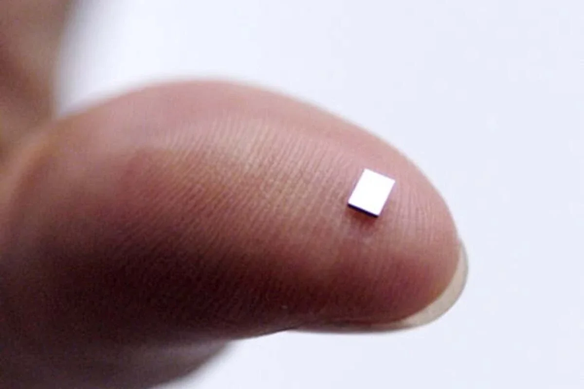
The new processor reaches a size of 0.7 nanometers and concentrates nearly 100 billion transistors on a surface similar to that of a fingernail. The company believes this technology can be used in CPUs, GPUs, and other processors.
What the new chip of less than 1 nanometer from IBM is like
The new chip of less than 1 nanometer uses an architecture called Nanostack, developed from Nanosheet technology, currently present in 2 and 3 nanometer chips.
The main difference is that the transistors are stacked and staggered vertically using a simple dielectric link. Additionally, they incorporate a new system to manage electrical current and renewed materials to control the flow of electricity.
In this architecture, the transistors are no longer completely surrounded as they are with Nanosheet, but receive electrical power independently from the front and back.
What performance the new IBM chip offers
Thanks to this design, IBM managed to manufacture a 0.7 nanometer chip, equivalent to 7 angstroms.